Laser Processing of Victrex® APTIV® PEEK Film
Introduction
APTIV® PEEK film is a part of the product line APTIV® 1000 series films that are unfilled semi-crystalline films made from Victrex® PEEK polymer. APTIV PEEK is available in various surface finishes and thicknesses. The APTIV PEEK chosen for testing has a gloss finish and is 25µm thick. A diagram depicting APTIV PEEK is shown in Figure 1.APTIV PEEK is utilized in a wide array of applications ranging from electrical insulation, aerospace insulation, pressure sensitive tapes and sensor and acoustic speaker membranes. APTIV PEEK exhibits high heat resistance, broad chemical resistance, high strength and toughness, and stable electrical insulation properties. APTIV PEEK film is suitable for laser cutting and marking processes. Other laser processes, such as laser engraving, are not suggested as they are not conducive to the intended uses of this material in film form. The non-contact nature of laser processing allows applications to be processed with small features and fine geometry which might be difficult to achieve with traditional mechanical methods. Universal Laser Systems makes it simple to consistently and repeatedly process this material to a high degree of dimensional accuracy because the non-contact nature of laser processing eliminates material deformation during processing.
Laser Processing Notes
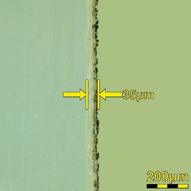
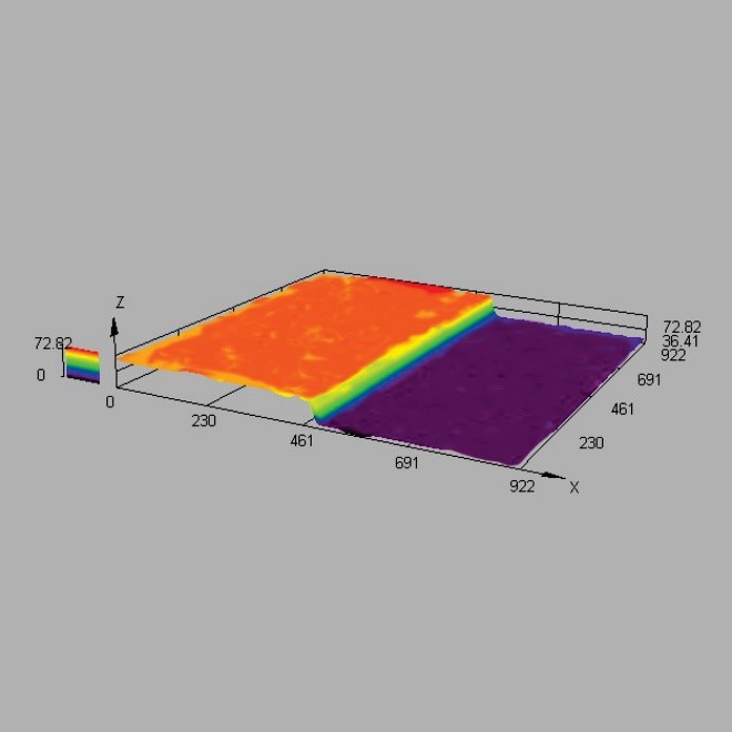
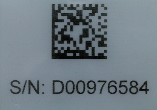
APTIV PEEK was tested to assess laser processing compatibility and determine the best configuration of laser peak power and wavelength. There was found to be no substantial difference between 9.3 and 10.6µm laser energy when used for the laser cutting of APTIV PEEK film. A microscopy image taken at 300x magnification of the edge of APTIV PEEK is shown in Figure 2. The 3D image in Figure 3 depicts how the processed edge of the PEEK film responds to laser cutting with the system configuration of a single 75 watt 9.3µm laser. APTIV PEEK readily absorbs the 1.06µm laser wavelength, Additionally, APTIV PEEK responds to laser marking with the system configuration of a single 1.06µm laser of either 40 or 50 watts, creating a high contrast mark on the surface of the material. This surface modification does not produce debris, and therefore does not require post-processing. An image of APTIV PEEK after laser marking is shown in Figure 4.Processing Examples
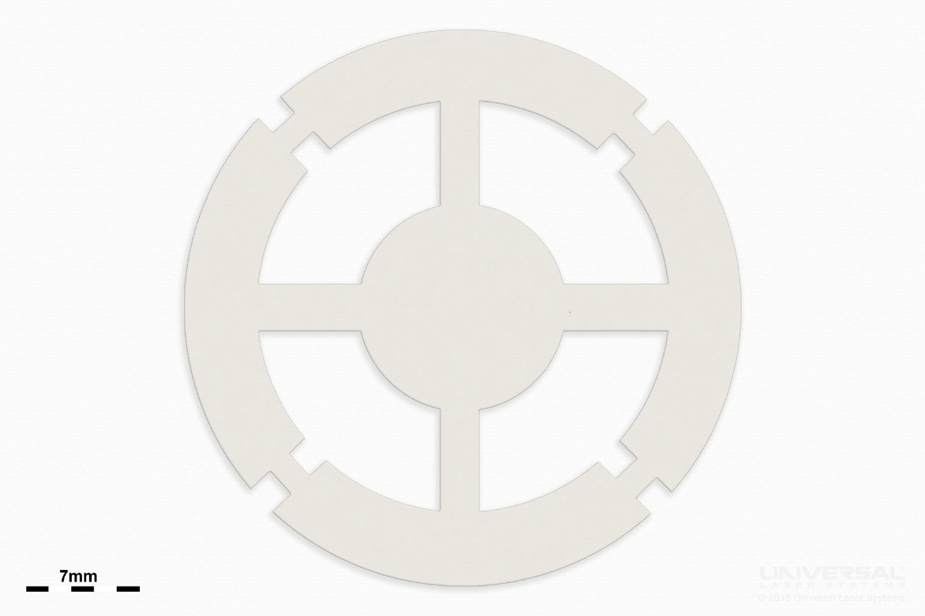
APTIV PEEK applications requiring fine geometry and intricate detail without degrading the physical properties of the material can be accomplished with Universal Laser Systems technology. An image of APTIV PEEK after laser marking is shown in Figure 4. An example demonstrating the results of laser cutting APTIV PEEK using the recommended system configuration is shown in Figure 5.Conclusion
APTIV PEEK is suitable for laser processing and was extensively tested to determine the optimal processing configuration. Through this testing it was determined that laser cutting is viable with this material and using a 75 watt CO2 laser source at either 9.3 or 10.6µm. APTIV PEEK efficiently absorbs the 9.3 and 10.6µm wavelengths of laser energy to produce a processed edge that has minimal heat-affected zone and discoloration. APTIV PEEK was also found to absorb 1.06µm laser energy which produces a high contrast surface mark, making laser marking of this material a viable process with either a 40 or 50 watt 1.06µm laser source.
APTIV® PEEK film is a part of the product line APTIV® 1000 series films that are unfilled semi-crystalline films made from Victrex® PEEK polymer. APTIV PEEK is available in various surface finishes and thicknesses. The APTIV PEEK chosen for testing has a gloss finish and is 25µm thick. A diagram depicting APTIV PEEK is shown in Figure 1.APTIV PEEK is utilized in a wide array of applications ranging from electrical insulation, aerospace insulation, pressure sensitive tapes and sensor and acoustic speaker membranes. APTIV PEEK exhibits high heat resistance, broad chemical resistance, high strength and toughness, and stable electrical insulation properties. APTIV PEEK film is suitable for laser cutting and marking processes. Other laser processes, such as laser engraving, are not suggested as they are not conducive to the intended uses of this material in film form. The non-contact nature of laser processing allows applications to be processed with small features and fine geometry which might be difficult to achieve with traditional mechanical methods. Universal Laser Systems makes it simple to consistently and repeatedly process this material to a high degree of dimensional accuracy because the non-contact nature of laser processing eliminates material deformation during processing.
Laser Processing Notes
APTIV PEEK was tested to assess laser processing compatibility and determine the best configuration of laser peak power and wavelength. There was found to be no substantial difference between 9.3 and 10.6µm laser energy when used for the laser cutting of APTIV PEEK film. A microscopy image taken at 300x magnification of the edge of APTIV PEEK is shown in Figure 2. The 3D image in Figure 3 depicts how the processed edge of the PEEK film responds to laser cutting with the system configuration of a single 75 watt 9.3µm laser. APTIV PEEK readily absorbs the 1.06µm laser wavelength, Additionally, APTIV PEEK responds to laser marking with the system configuration of a single 1.06µm laser of either 40 or 50 watts, creating a high contrast mark on the surface of the material. This surface modification does not produce debris, and therefore does not require post-processing. An image of APTIV PEEK after laser marking is shown in Figure 4.
APTIV PEEK applications requiring fine geometry and intricate detail without degrading the physical properties of the material can be accomplished with Universal Laser Systems technology. An image of APTIV PEEK after laser marking is shown in Figure 4. An example demonstrating the results of laser cutting APTIV PEEK using the recommended system configuration is shown in Figure 5.Conclusion
APTIV PEEK is suitable for laser processing and was extensively tested to determine the optimal processing configuration. Through this testing it was determined that laser cutting is viable with this material and using a 75 watt CO2 laser source at either 9.3 or 10.6µm. APTIV PEEK efficiently absorbs the 9.3 and 10.6µm wavelengths of laser energy to produce a processed edge that has minimal heat-affected zone and discoloration. APTIV PEEK was also found to absorb 1.06µm laser energy which produces a high contrast surface mark, making laser marking of this material a viable process with either a 40 or 50 watt 1.06µm laser source.


